CAP.01
New board design
Schematic capture, component libraries, placement, and layout for a design that starts as a blank sheet — built on a clean, maintainable Altium project.
PCB LAYOUT / ALTIUM DESIGNER / CLI SYSTEMS
We design and rescue printed circuit boards in Altium Designer — multilayer, rigid-flex, and high-speed work delivered as a complete manufacturing package. Existing project or blank canvas, we route it like it's going to production. Because it is.
Who we are
AltiumDeveloper is the PCB design practice of CLI Systems. We take on the boards that need to actually work in the field — not entry-level, not hacked together, not "close enough."
Bring us a brand-new design and we'll carry it from schematic capture through layout, verification, and a fabrication-ready package. Bring us an existing Altium project that stalled, needs a respin, or needs cleaning up, and we'll pick it up mid-stream and finish it right.
Either way you get real design files, sane libraries, and documentation your fab and assembly house can build from without a dozen back-and-forth emails.
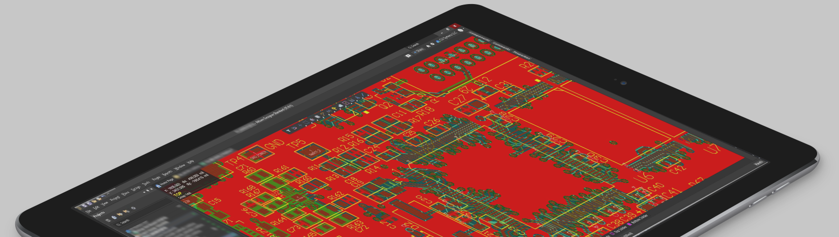
What we do
A full-stack design service. Whatever technology your product needs, it's a routing problem we've solved before.
Schematic capture, component libraries, placement, and layout for a design that starts as a blank sheet — built on a clean, maintainable Altium project.
Inherited a stalled or messy Altium project? We pick it up mid-stream, resolve the DRC and library debt, run the ECOs, and get it back to buildable.
Controlled stackups, plane management, and high-density interconnect — blind and buried vias, microvias, and via-in-pad where the density calls for it.
Dynamic and static bends, coverlay, stiffeners, and bend-aware routing for boards that have to fold into a real enclosure and survive it.
Controlled impedance, differential pairs, length and skew matching, return-path discipline, and EMI-aware layout for the signals that actually care.
Gerber / ODB++ / IPC-2581, drill files, BOM, assembly drawings, pick-and-place, and a DFM review — a package your fab can build without guessing.
Selected work
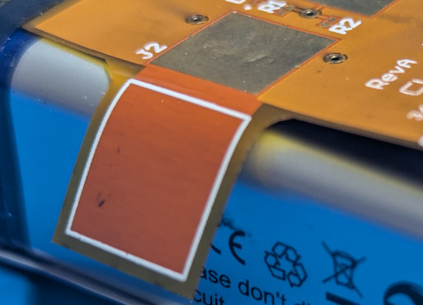 FLEX · CUSTOM
We helped a client develop a custom flex PCB to integrate into an existing system for voltage monitoring application — folded into the assembly working with the existing enclosure.
The board carries multiple bends, 0402 passives, and was designed for a 10,000-unit production run from the start.
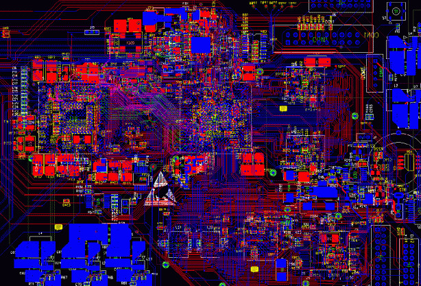 LAYOUT · ALTIUM
Tight placement, poured planes, and disciplined routing on a densely packed board — analog kept clean, digital kept contained, and every net length-aware where it mattered.
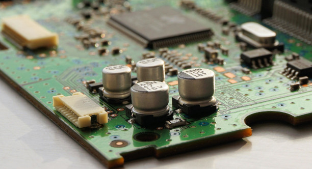 ASSEMBLY · RIGID
Several rigid boards designed to work as one system, joined by flex jumpers through board-to-board connectors — each board routed to its own mechanical envelope, with the interconnect planned so the stack folds together and builds cleanly every time.
How it works
We go through the netlist, constraints, stackup, and mechanical envelope, and agree on DFM targets before a single trace is drawn.
Placement, plane strategy, controlled impedance, and length tuning — with checkpoints so you see the board take shape, not just the final file.
Clean DRC, a DFM / DFA pass, and impedance and fabrication details confirmed against your chosen manufacturer's capabilities.
You get the full manufacturing package plus the source Altium project — version-controlled, documented, and yours to keep.
Get in touch
New design, respin, or a project that needs rescuing — send the details and we'll come back quickly with next steps. We promise to respond fast.